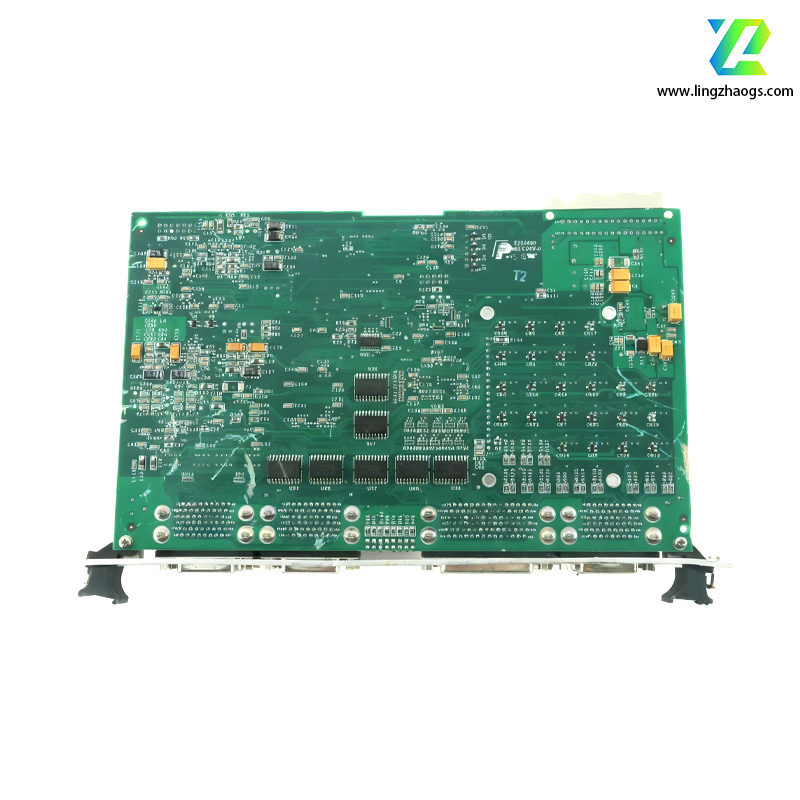
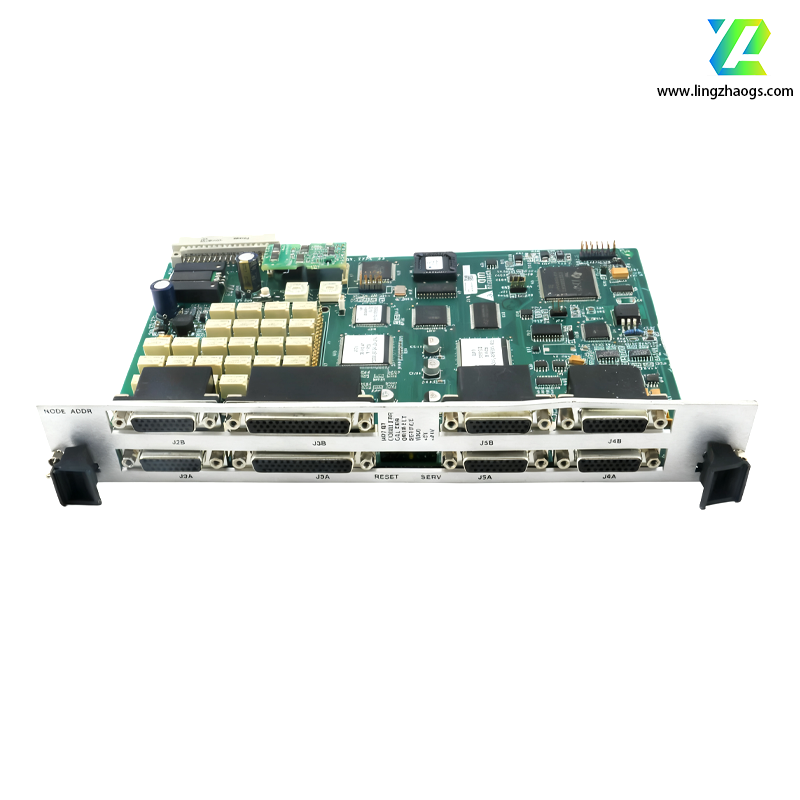
The LAM 810-082745-003 is a specialized printed circuit board (PCB) or control module designed for critical signal routing, edge detection, and process control in semiconductor manufacturing equipment. As with many LAM Research components, detailed official specifications are restricted to authorized customers. However, the following insights are derived from industry context, compatible product lines, and third-party technical resources.
- Edge Detection & Signal Conditioning: Optimized for precise wafer edge detection in plasma etching, deposition, or metrology systems. Integrates sensors and analog/digital converters to ensure micron-level accuracy in wafer alignment.
- RF Signal Management: Supports high-frequency signal routing (e.g., 58–60 MHz) for plasma generators, minimizing EMI/RFI interference in sensitive environments.
- Modular Interface: Features configurable I/O ports for connecting to actuators, sensors, and control systems (e.g., wafer stage drives, gas flow controllers).
Precision Edge Detection
- Utilizes laser-based or capacitive sensors to identify wafer edges, enabling accurate alignment during etching or deposition processes.
- Real-time feedback loop ensures <10 μm positional error tolerance.
RF Signal Integrity
- Shielded traces and impedance-matched circuitry reduce signal degradation in high-frequency plasma environments.
- Supports 50 Ω/75 Ω impedance for coaxial cable connections.
Industrial Communication
- Protocol Support: Ethernet/IP, RS-485, or SPI for integration with LAM’s Sense.i™ process control platform.
- Diagnostic Tools: Built-in LED indicators for power, sensor status, and communication errors.
Safety & Reliability
- Overvoltage/Undervoltage Protection: Rapid shutdown (<5 ms) to prevent damage from power fluctuations.
- Redundant Design: Optional dual-channel configuration for fault tolerance in mission-critical applications.
- Plasma Etching Systems (e.g., LAM Vantex™): Ensures precise wafer positioning during 3D structure patterning (e.g., FinFET, GAAFET).
- Chemical Vapor Deposition (CVD): Controls wafer alignment for uniform thin-film deposition in memory chip production.
- Metrology Equipment: Enables edge inspection and defect detection in advanced packaging processes (e.g., 3D IC stacking).
- Wafer Handling Robotics: Provides feedback for robotic arms to transfer wafers between chambers in cleanroom environments.
- Equipment Compatibility: Designed for LAM Research’s 2300 Series, 3900 Series, and select legacy tools.
- Software Tools: Configurable via LAM’s Workbench or MyLam portal for parameter tuning and firmware updates.
- Third-Party Support: Available through authorized distributors (e.g., Saulabb) for maintenance and replacement.
- Technical Resources: Official datasheets and user manuals are restricted to LAM Research customers. Third-party distributors may provide limited specifications.
- Warranty: Standard 12-month warranty; extended coverage available for critical applications.
This module plays a pivotal role in enabling high-yield semiconductor manufacturing by ensuring process consistency and minimizing wafer misalignment. Its design aligns with LAM Research’s focus on energy efficiency and sustainable production, supporting next-generation chip technologies (e.g., 2 nm nodes).
For exact technical details or procurement inquiries, contact LAM Research directly or their authorized partners.