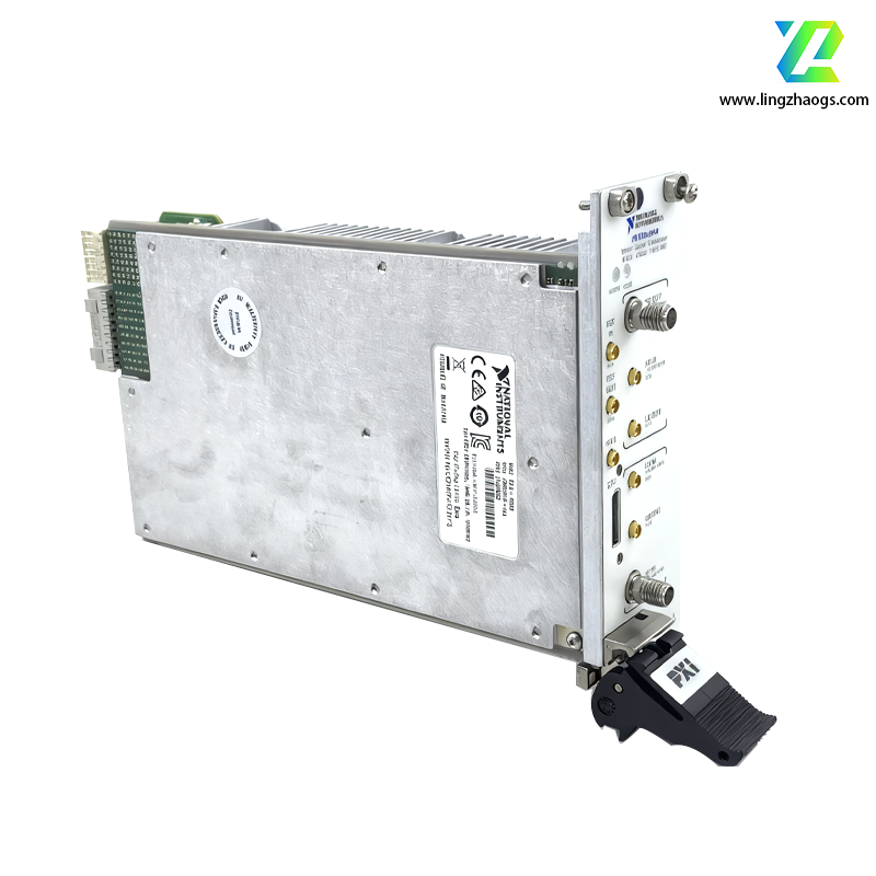
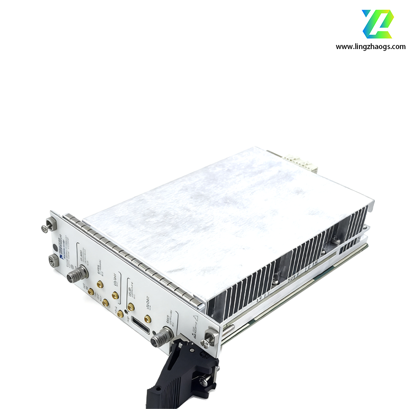
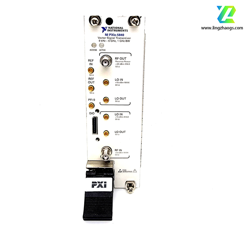
The NI PXIe-5840 is a high-performance Vector Signal Transceiver (VST) designed for the PXI Express (PXIe) bus architecture, belonging to National Instruments (NI)’s flagship RF test product line. It integrates a 6 GHz vector signal generator (VSG) and a 6 GHz vector signal analyzer (VSA) into a single modular unit, plus a programmable FPGA for real-time signal processing. This all-in-one design eliminates the need for separate instruments, reducing system complexity and latency—making it ideal for demanding RF testing scenarios such as 5G NR FR1 (Sub-6 GHz) conformance testing, radar system validation, and semiconductor RFIC characterization.
- Module Series: PXIe Vector Signal Transceiver (VST), optimized for integrated RF transmit/receive testing
- Part Number: 783149-01 (standard model); 783149-02 (extended temperature model)
- Physical Dimensions: 2-slot 3U PXIe form factor, 20.3 cm × 16.0 cm (width × length)
- Weight: Approximately 1.8 kg (3.97 lbs)
- Power Requirements:
- +3.3 V DC (3.0 A)
- +12 V DC (4.5 A)
- -12 V DC (0.8 A)
- Power Consumption: Typical 60 W, Maximum 80 W
- Interface Type:
- PXIe x8 lane (up to 8 GB/s data transfer rate) for high-speed waveform uploads/downloads
- 2 SMA female connectors (RF Tx: transmit output; RF Rx: receive input)
- 1 SMA female connector (External LO I/O) for frequency extension/synchronization
- 1 26-pin D-Sub connector (Auxiliary I/O) for trigger signals and clock reference
- 1 USB 3.0 port (for local FPGA configuration and debugging)
- Operating Temperature Range:
- Commercial grade: 0°C ~ 55°C
- Extended grade (783149-02): -40°C ~ 85°C (for harsh aerospace/defense environments)
- Environmental Ratings:
- Shock Resistance: 50 g peak (11 ms duration, half-sine)
- Vibration Resistance: 5 g RMS (10 Hz ~ 500 Hz, random)
- Ingress Protection: IP30 (prevents solid foreign object intrusion)
- Compliance: Meets FCC Part 15 Class A, CE EN 61326-1, UL 61010-1, and IEC 61010-1 safety & EMC standards
- Frequency Range: 9 kHz ~ 6 GHz (continuous coverage, no gaps)
- Output Power:
- Minimum: -140 dBm (typical, at 1 GHz)
- Maximum: +20 dBm (typical, at 1 GHz, into 50 Ω)
- Power Resolution: 0.1 dB
- Signal Fidelity:
- Spurious-Free Dynamic Range (SFDR): ≥75 dBc (1 GHz carrier, 10 MHz bandwidth, typical)
- Phase Noise: -120 dBc/Hz (1 GHz carrier, 10 kHz offset, typical)
- Harmonic Distortion: ≤-60 dBc (2nd harmonic, 1 GHz, +10 dBm output)
- DAC Specifications:
- Resolution: 14-bit
- Real-Time Sampling Rate: 2.5 GS/s (supports up to 1 GHz real-time bandwidth)
- Waveform Memory: 1 GB (onboard, for storing custom arbitrary waveforms)
- Frequency Range: 9 kHz ~ 6 GHz (continuous coverage, no gaps)
- Input Power Handling:
- Maximum Safe Input Power: +20 dBm (100 mW)
- Damage Level: +30 dBm (1 W, 1 minute)
- Noise Performance:
- Noise Figure (NF): ≤10 dB (1 GHz, 10 MHz bandwidth, typical)
- Input-Referred Noise: -174 dBm/Hz (typical, at room temperature)
- Dynamic Range:
- Spurious-Free Dynamic Range (SFDR): ≥70 dBc (1 GHz, 10 MHz bandwidth, typical)
- Third-Order Intercept Point (IP3): +12 dBm (typical, at 1 GHz)
- ADC Specifications:
- Resolution: 14-bit
- Real-Time Sampling Rate: 2.5 GS/s (supports up to 1 GHz real-time bandwidth)
- Anti-Aliasing Filter: 80 dB/octave roll-off (prevents frequency aliasing)
- FPGA Chip: Xilinx Kintex UltraScale KU040 (1.1 M logic cells, 4.9 Gbps transceivers)
- Real-Time Processing Capabilities:
- Custom digital signal processing (DSP): Filtering, downconversion, demodulation, and error correction
- Low-latency control loops (≤1 µs) for closed-loop testing (e.g., beamforming, adaptive modulation)
- Support for MIMO (Multiple-Input Multiple-Output) testing (up to 8x8 MIMO with multiple VSTs)
- FPGA Programming Tools: LabVIEW FPGA Module (for graphical programming) and Xilinx Vivado (for HDL programming)
- Time Alignment: Tx and Rx channels are phase-aligned to within ±1 ns (enabling precise stimulus-response testing, e.g., antenna calibration)
- Clock Synchronization:
- Internal: 100 MHz OCXO (Oven-Controlled Crystal Oscillator), stability ±0.01 ppm/year
- External: 10 MHz reference input (via Auxiliary I/O) or PXIe backplane clock (for multi-module synchronization)
- Trigger Options:
- RF Trigger: Trigger on Tx/Rx signal thresholds (e.g., 5G NR preamble detection)
- Digital Trigger: TTL-compatible edge trigger via Auxiliary I/O or PXIe trigger lines (PXIe_Trig 0~7)
- Software Trigger: API-initiated trigger for automated test sequences
- Wireless Standards: 5G NR (FR1), LTE/LTE-A, Wi-Fi 7 (802.11be), Bluetooth 5.4, Zigbee, LoRaWAN, and satellite (DVB-S2X)
- Modulation Formats:
- Phase/Amplitude: BPSK, QPSK, 8PSK, 16QAM, 64QAM, 256QAM, 1024QAM, 4096QAM
- Frequency: FSK, GFSK, MSK
- Spread Spectrum: DSSS, OFDM (with up to 4096 subcarriers)
- Modulation Quality: Error Vector Magnitude (EVM) ≤ 0.5% (for QPSK, 1 GHz carrier, typical)
- Frequency Extension: External LO input (up to 20 GHz) for testing signals beyond 6 GHz (e.g., 77 GHz automotive radar with a downconverter)
- Signal Conditioning: Compatible with NI PXIe-5691 (RF preamplifier) and NI PXIe-2543 (RF multiplexer) for weak signal detection and multi-DUT testing
- Antenna Integration: Works with NI PXIe-5680 (RF switch matrix) and third-party antennas for over-the-air (OTA) testing
- Core Drivers & Software:
- NI-RFmx Measurement Suite: For standard-based measurements (e.g., 5G NR ACLR, Wi-Fi 7 EVM)
- NI-VST Driver: For low-level hardware control (Tx/Rx configuration, FPGA interface)
- LabVIEW 2022+: For custom test program development, FPGA programming, and GUI design
- NI TestStand: For test sequence automation, data logging, and report generation (e.g., production line testing)
- Programming Compatibility:
- NI Ecosystem: Native support for LabWindows/CVI and Measurement Studio
- Third-Party Languages: C/C++, C#, Python (via NI-RFmx Python bindings), and MATLAB (via NI-RFmx Toolbox)
- Scripting: Python/LabVIEW scripting for rapid prototyping (e.g., batch testing of 5G UE modules)
- Calibration Tools:
- Built-in automated calibration (via NI-VST) for gain, phase, and linearity correction
- Recommended Calibration Interval: 1 year (or after major temperature changes)
- External Calibration: Supported via NI Calibration Services (ISO 17025 accredited)
The NI PXIe-5840’s integrated design and high performance make it ideal for:
- 5G NR FR1 Testing: 5G UE/base station conformance testing (e.g., EVM, ACLR, channel power) and OTA beamforming validation
- Aerospace & Defense: Radar system testing (pulsed, FMCW, phase-coded radar), satellite communication (SATCOM) link analysis, and electronic warfare (EW) signal simulation/analysis
- Semiconductor RFIC Testing: Wafer-level and package-level testing of 5G RF transceivers, power amplifiers (PAs), and low-noise amplifiers (LNAs)
- Wireless Infrastructure: Wi-Fi 7 access point (AP) testing, Bluetooth 5.4 module calibration, and industrial IoT (IIoT) sensor validation
- Automotive Electronics: V2X (Vehicle-to-Everything) communication testing (C-V2X, DSRC) and 77 GHz radar sensor signal emulation (with external downconverter)
- Ideal Use Cases: Applications requiring integrated 6 GHz RF transmit/receive, 1 GHz real-time bandwidth, and low-latency FPGA processing; suitable for R&D, conformance testing, and high-volume production
- Comparison with Similar VSTs:
- vs. NI PXIe-5830: PXIe-5840 offers 6 GHz frequency range (vs. 3 GHz) and 1 GHz bandwidth (vs. 500 MHz); choose for higher-frequency, wider-bandwidth testing
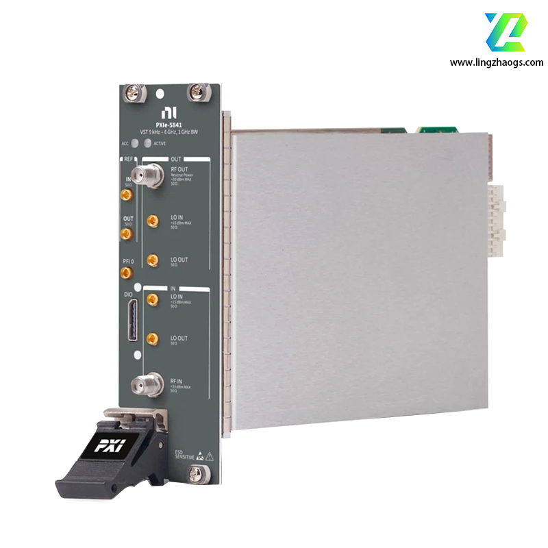
- vs. NI PXIe-5841: PXIe-5840 has lower frequency (6 GHz vs. 26.5 GHz) but lower cost; ideal for Sub-6 GHz 5G/Wi-Fi 7 testing
- System Compatibility:
- Chassis: Requires NI PXIe chassis with 2 available slots and PXIe x8 lanes (e.g., PXIe-1085, PXIe-1075) or third-party PXIe-compliant chassis
- Companion Modules:
- OTA Testing: Pair with NI PXIe-5680 (switch matrix) and anechoic chambers for 5G OTA validation
- Power Measurement: Integrate with NI PXIe-4154 (SMU) for RFIC power consumption testing
- Temperature Control: Use NI PXIe-6358 (DAQ) to monitor DUT temperature during testing
- Limitations: No built-in millimeter-wave (mmWave) support (requires external upconverters for FR2 testing); higher cost than discrete VSG/VSA systems (justified by reduced complexity)
- Alternative Models:
- Lower Cost: NI PXIe-5830 (3 GHz, 500 MHz bandwidth)
- Higher Frequency: NI PXIe-5841 (26.5 GHz, 2 GHz bandwidth)
- Entry-Level: NI PXIe-5632 (VSA) + NI PXIe-5673 (VSG) (discrete solution for budget-sensitive tasks)